Select your location:

Country

Clean room robot solutions for semiconductor manufacturing

KUKA technologies and robotics for cleanroom device manufacturing meet the high requirements for purity, cleanliness and functionality in semiconductor manufacturing. They combine extreme agility and maximum precision – even with short cycle times.


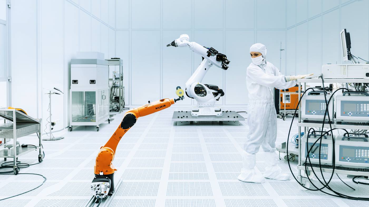
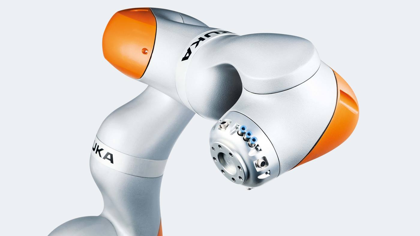
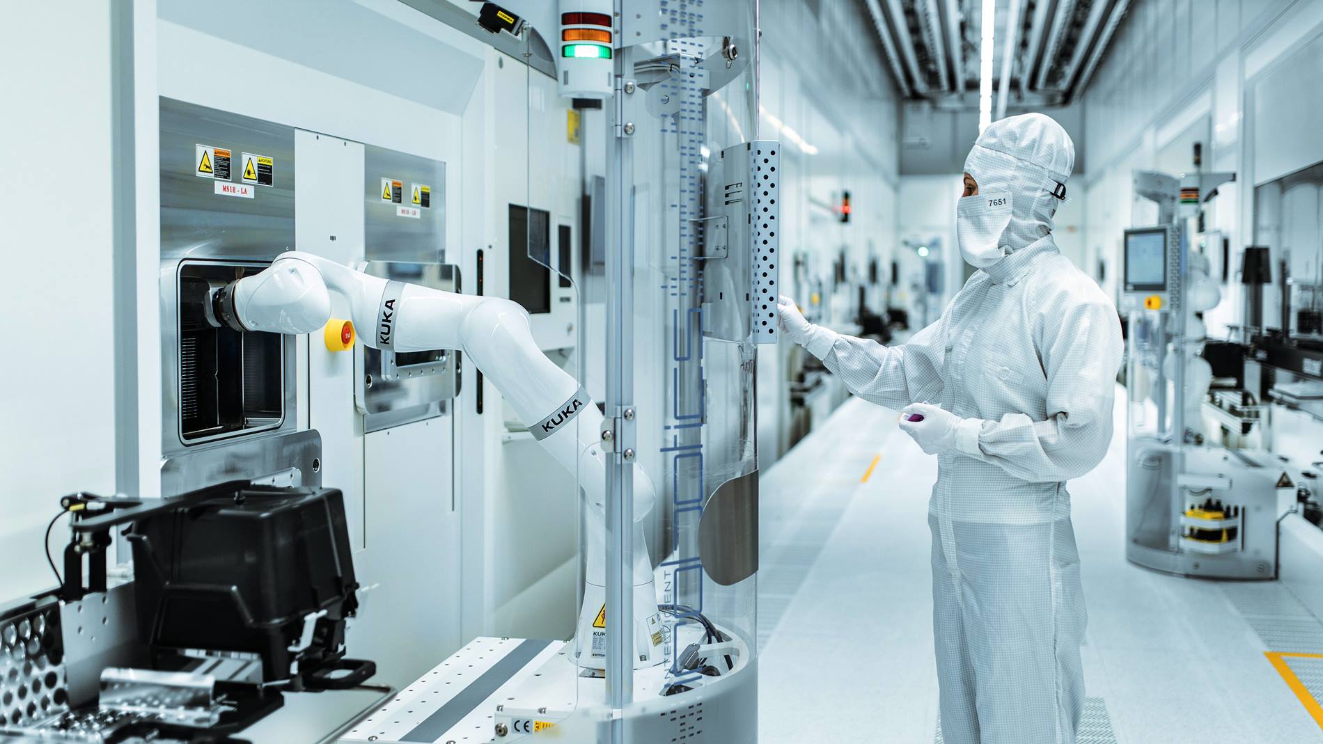
Designed for the stringent clean working requirements of the semiconductor industry: KUKA places particular emphasis on cleanrooms and facility safety.

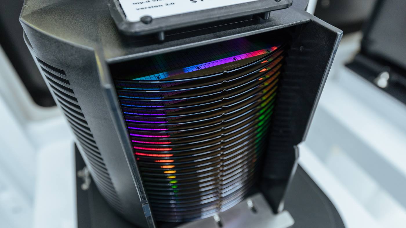
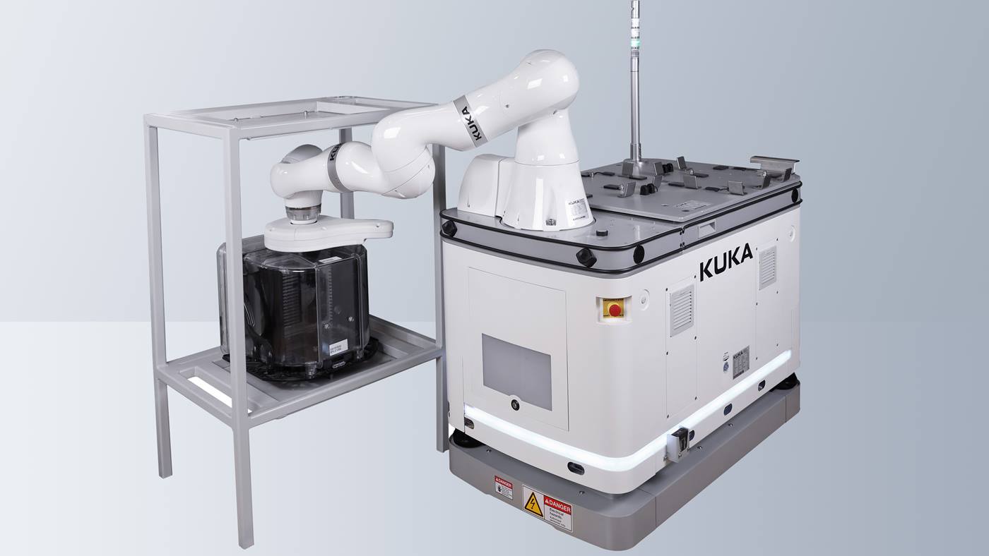
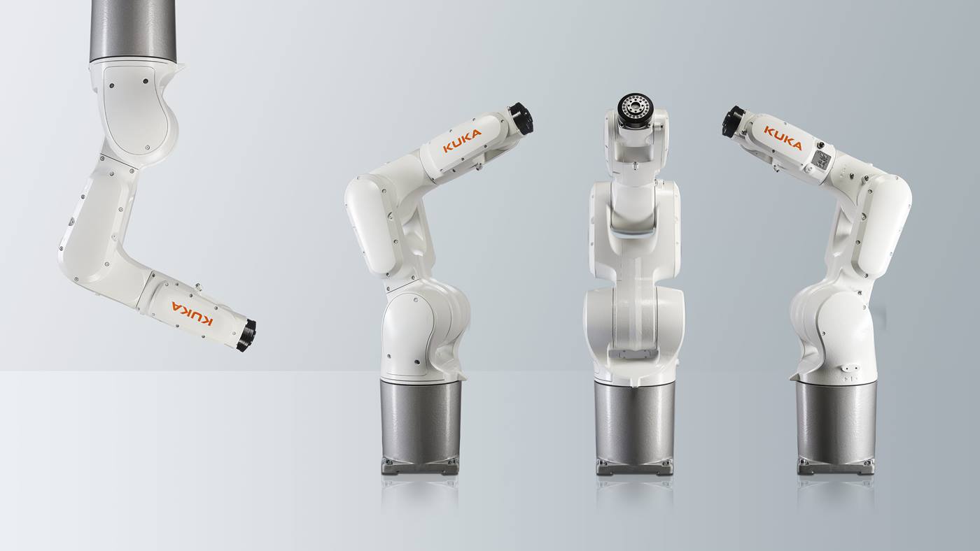
Especially for cleanroom manufacturing, KUKA offers low-particle and low-emission robots, cobots, and platforms for the manufacture and safe handling of highly sensitive microelectronic devices, such as chips and semiconductors. Even our own production facility operates under this strict cleanroom environment.

Together with system partners, KUKA supplies future-proof Industrie 4.0 solutions for the semiconductor industry with perfectly matched hardware and software meeting the demands of networking capability and manufacturing flexibility.

Humans and robots in ultra-clean room production environment: highly automated semiconductor manufacturing factories of the future.

Cleaner than in operating rooms: mass production of semiconductor chips in a cleanroom environment up to category 1 at Infineon GmbH.

Robot technology for semiconductor device manufacturing from a single supplier

  • Robotics in cleanroom design

    Clean room robots and (mobile) cobots with a high cleanroom classifications – for example, thanks to internally-located, encapsulated guide mechanisms and cables as well as integrated drive technology


  • Software for mobile applications

    Intelligent, SEMI SECS-compliant software packages, specific to semiconductor manufacturing.

  • Engineering & Customer Service

    We offer customized, application-specific packages to meet your requirements.
  • KUKA TechCenters around the world with global standards

    KUKA TechCenters are available to customers as test laboratories at various  facility locations, including in Taiwan and China.

Tailored to cleanrooms from head to toe: industrial robots for semiconductor manufacturing and mobile cobots from KUKA.

Precise and fast robots of a high cleanroom class: greater safety through additional certification by the Fraunhofer Institute (ISO 14644-1)

Cleanroom-relevant criteria are already taken into account during the development of our robots Given their high ISO class, our standard robots are thus already suitable to integrate into many cleanroom applications.

 They have special, easy-to-clean surfaces as well as special primer coatings, seals and paint finishes on every axis. As standard, they are ESD-compatible and tested by Fraunhofer IPA for cleanroom suitability.

Cleanroom equipment is essential for the production of silicon wafer discs

Fraunhofer IPA is one of the world’s leading institutes in the fields of ultraclean production and contamination control. We have been work closely with KUKA for over 18 years. Firstly in the context of the Fraunhofer Tested Device® and CSM® cleanroom certifications, and also with a view to the design of robots to meet cleanliness requirements.

Dr. Frank Bürger, Fraunhofer IPA

Mobile cobots for clean room manufacturing: the safe handling of sensitive components.

The industrial manufacturing enviroment of tomorrow requires mobile production and logistics concepts which are intelligently networked, modular and versatile.
Mobile cleanroom cobots (KMR iiwa) guarantee the safe transportation and handling of sensitive components, such as wafers, chips, masks and carriers from one process to the next. They can navigate a facility in all directions autonomously and without the need to integrate safety fencing.

Increased productivity for semiconductor manufacturing

KUKA mobile cleanroom cobot handles wafer cassettes safely, flexibly and without recharging interruptions.

White paper: Next-level automation with KUKA robotics for cleanrooms

Read more about the future of semiconductor fabrication in the free white paper 

Download PDF

KUKA TechCenter test laboratories: from custom-tailored test to complete solutions for integration in the field of mobility

We carry out comprehensive and custom-tailored tests for semiconductor manufacturing as well as within the electronics device industry in international test facilities for our customers. Depending on the project, application and requirement, we offer everything from feasibility studies, interface tests and 24-hour test runs all the way to a finished product.

You need an individual solution?

Utilizing our expertise and experience, we would be happy to advise you and work with you to find the perfect solution to  your specific manufacturing challenges.

Looking for automation partners?

Leverage our worldwide partner network in the electronics industry