Select your location:

Country

Cobots: the new form of wafer handling in cleanrooms 

Cobots are entering the cleanrooms of the electronics industry. In wafer handling, they score high with customers for their reliability as well as top quality and safety standards. Cobots thus take automation in cleanrooms to a new level.


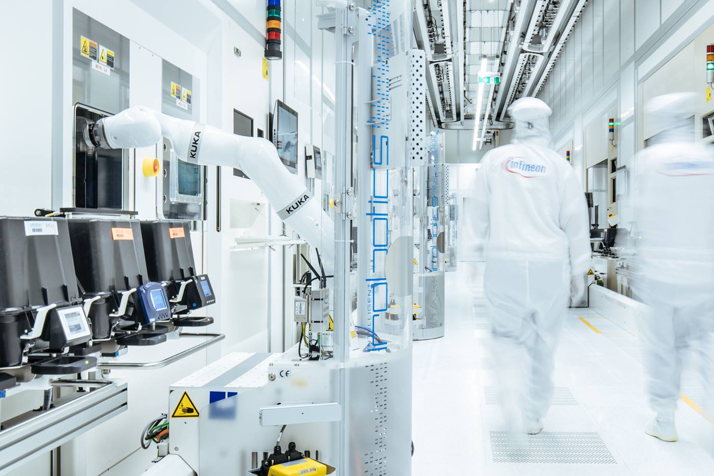
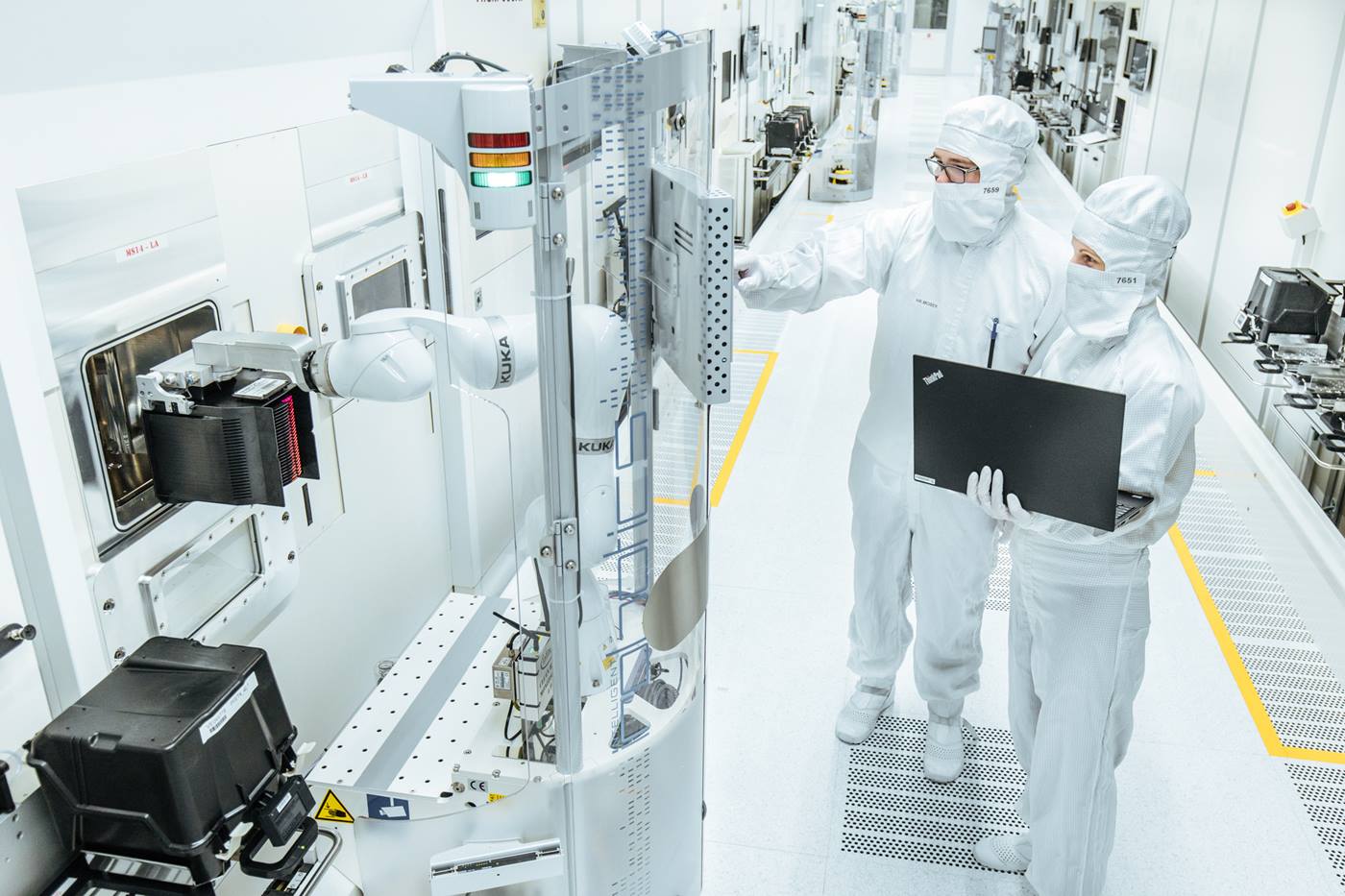
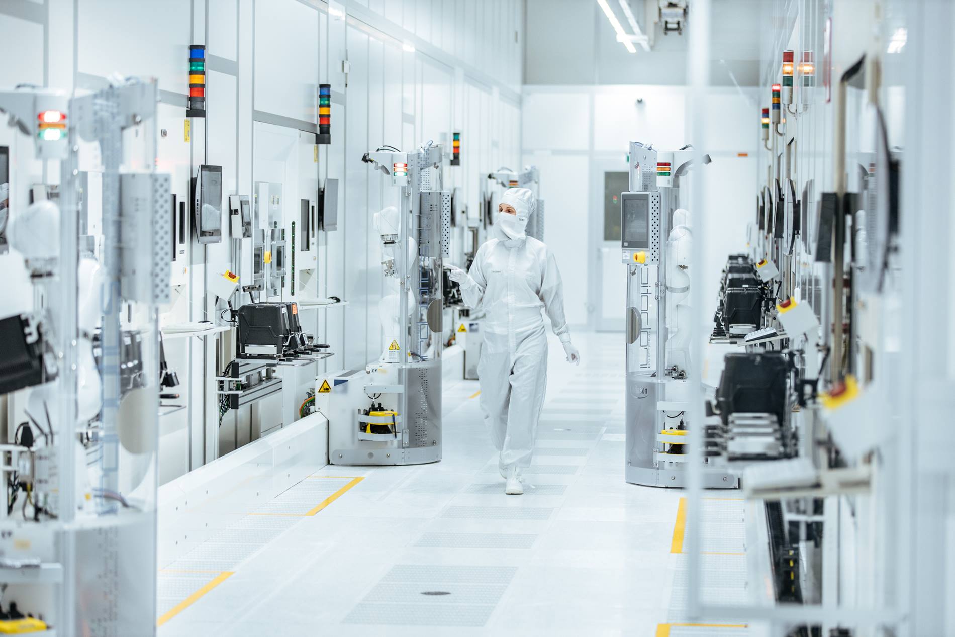
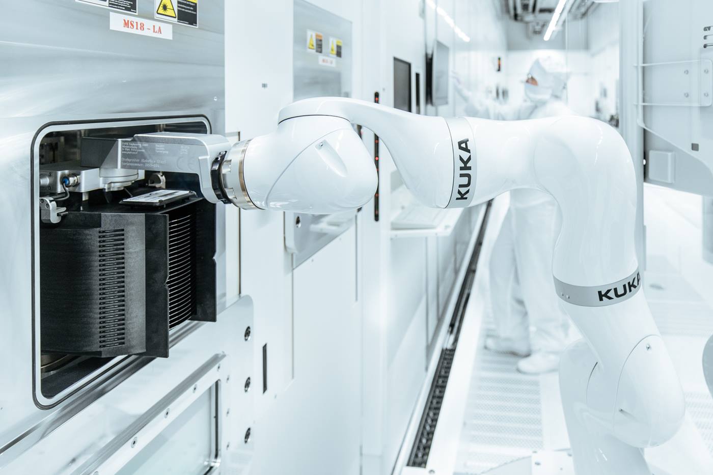
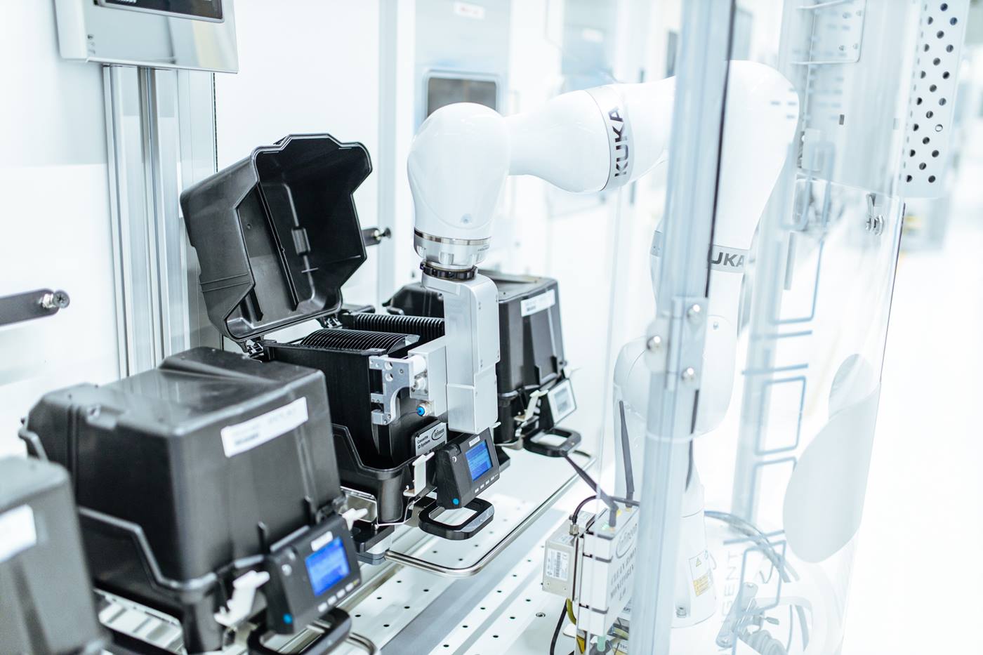
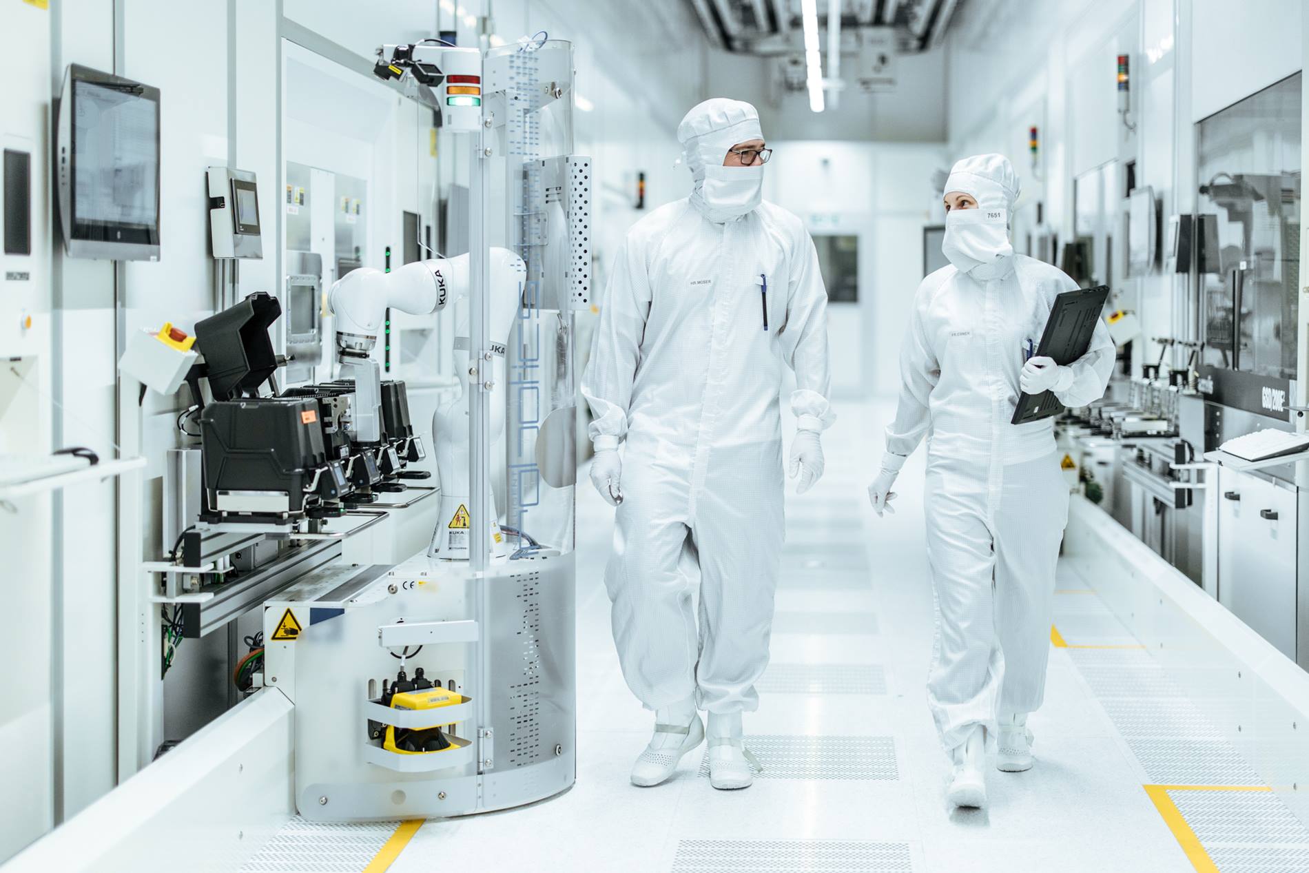
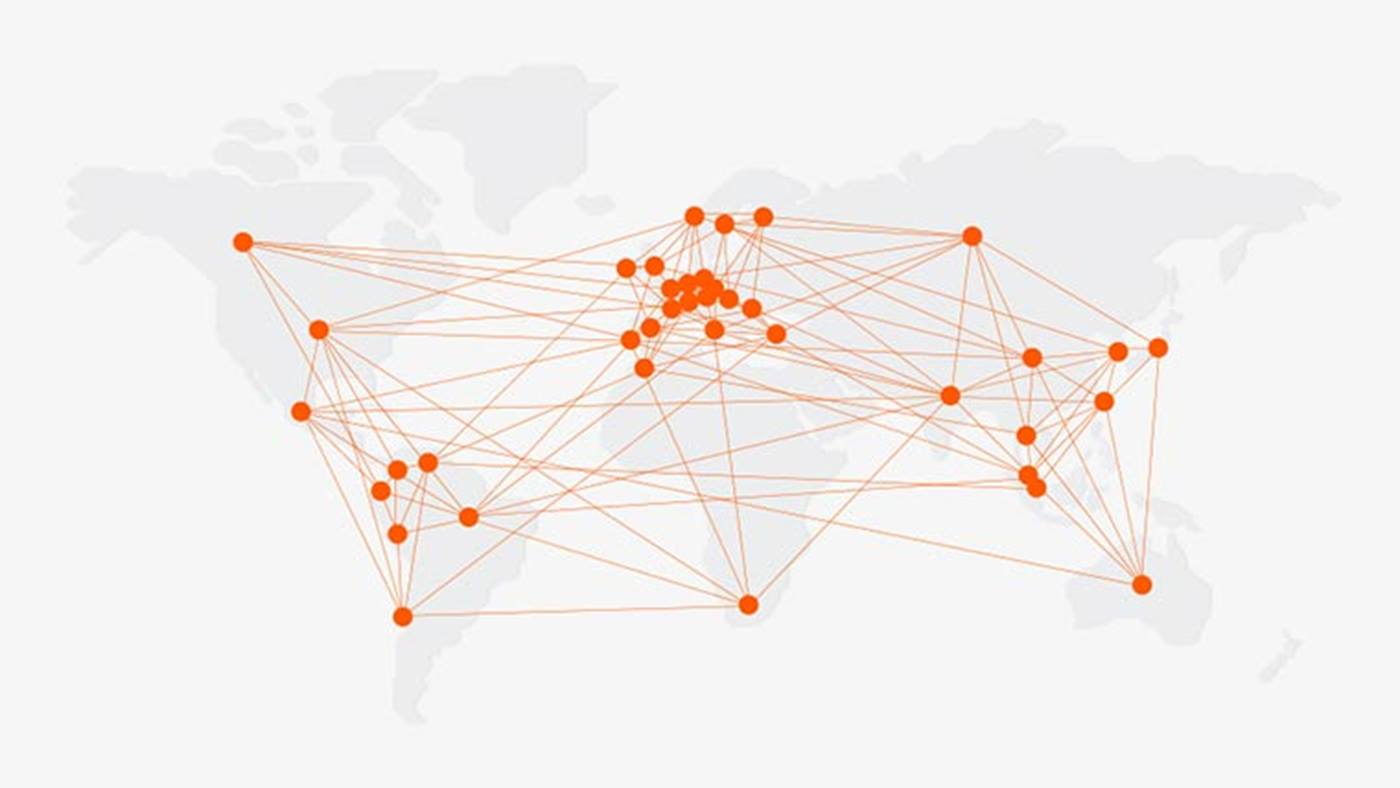
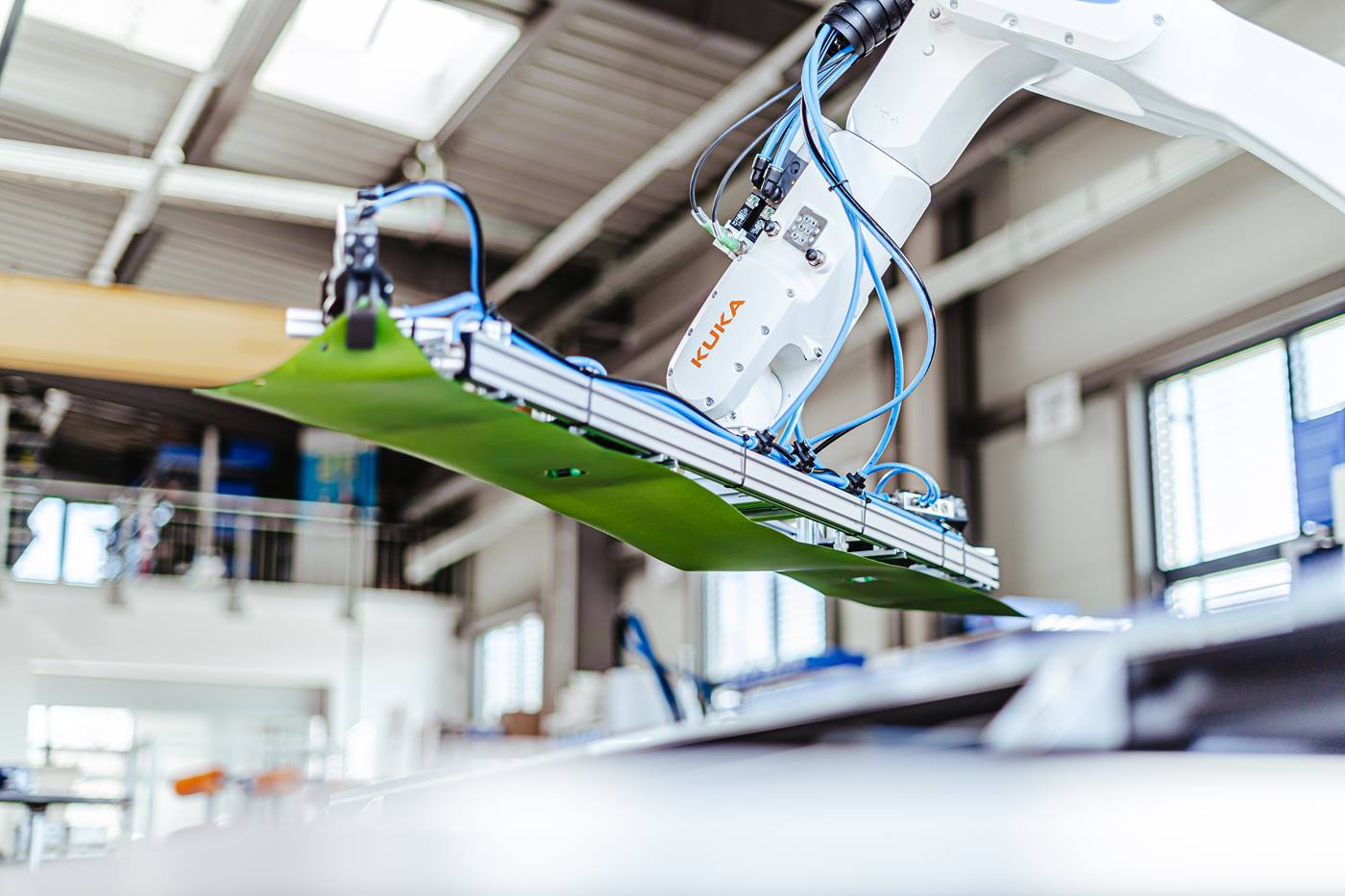
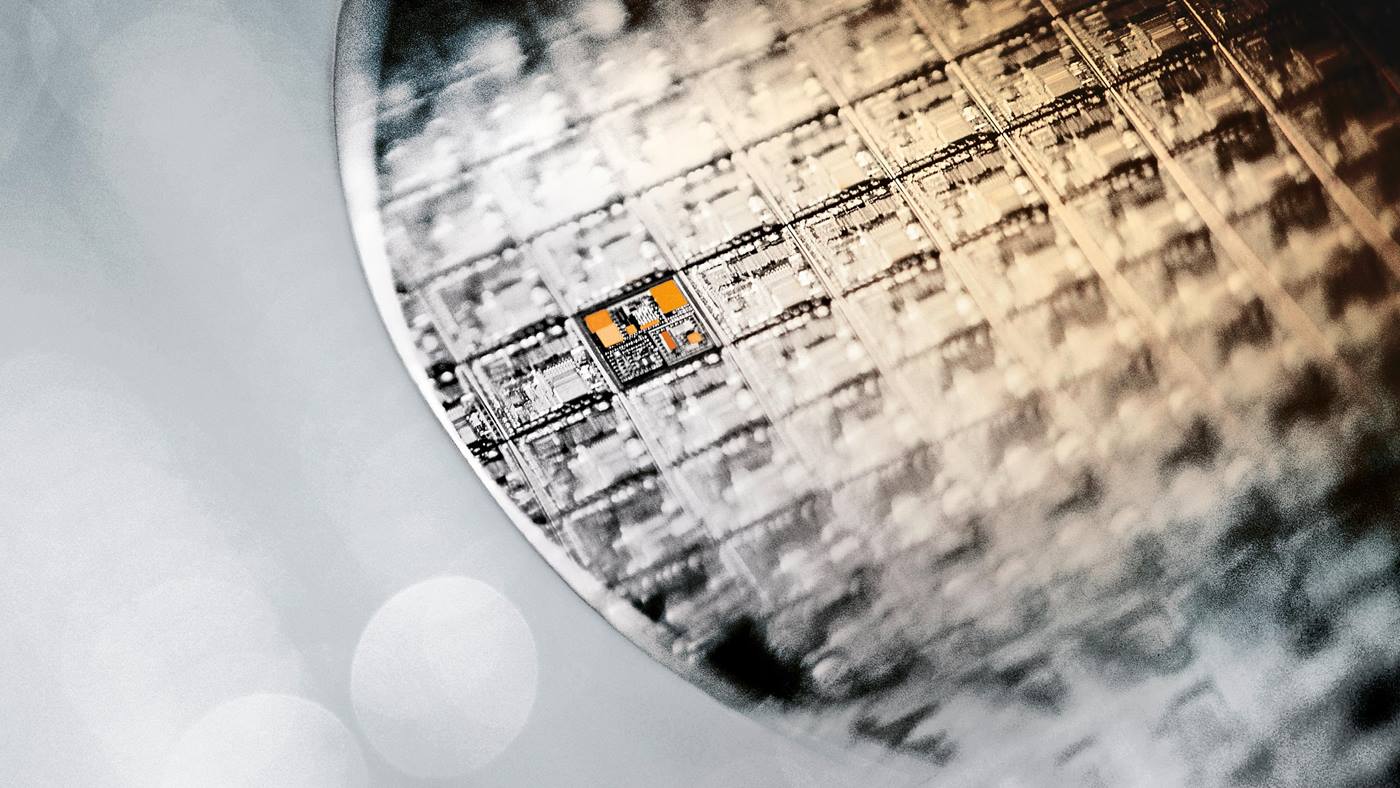
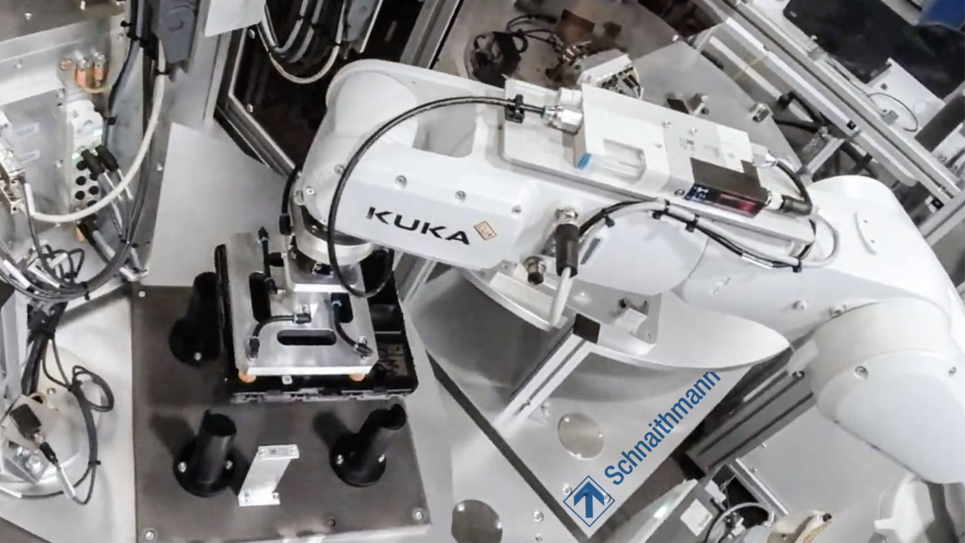
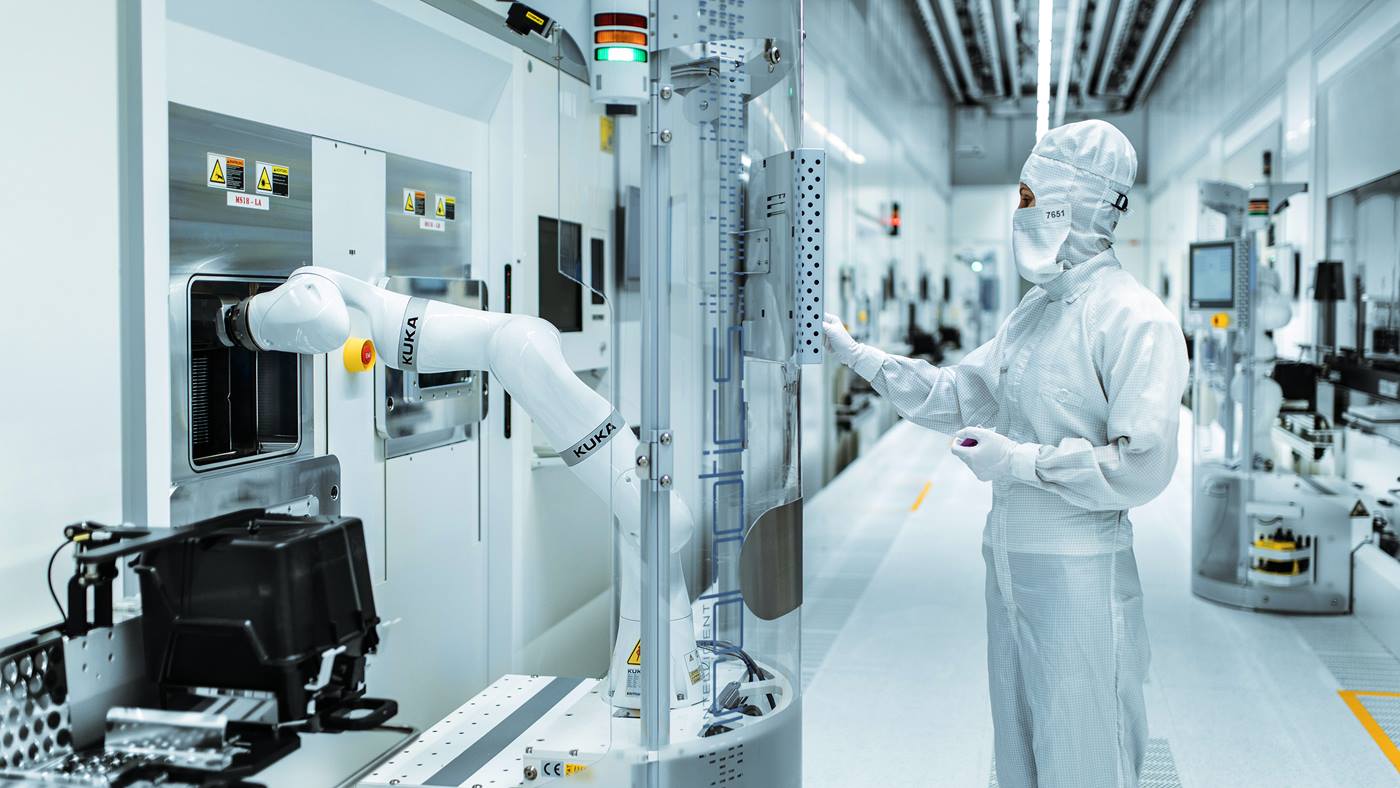
At the plant of KUKA customer Infineon, 17 sensitive wafer handling robots ensure efficiency and safety

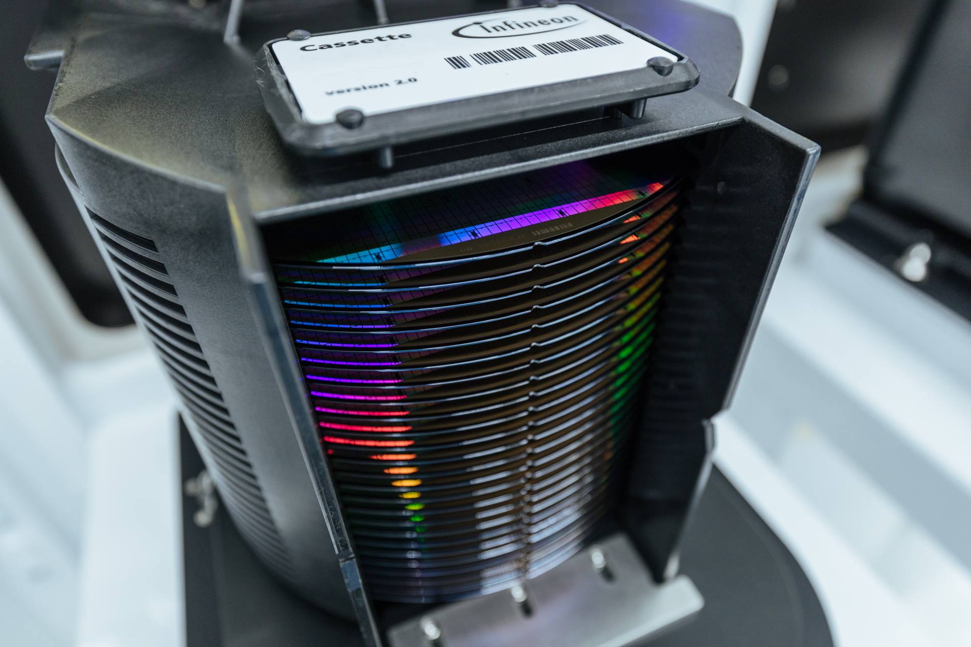
No, silicon wafers are not really a collaborative product: measuring as little as 40 micrometers in thickness, many silicon wafers are thinner than a hair and yet have a diameter of 150 to 300 millimeters, which is roughly the size of a pizza. This highly fragile material cannot be picked up by hand. To turn these sensitive silicon wafers – a cassette full of which can have the value of a mid-range car – into chips, they must pass through up to 1,200 process steps during fabrication. And, for each of these, they need to be transferred to a different automated processing station. A clear case for a robot like the LBR iiwa CR. These power semiconductors – used, for example, in cars, smartphones, refrigerators or in server farms and the traction units of locomotives – are produced at the Infineon site in Villach, Austria.

Each cassette full of the sensitive silicon wafers can have the value of a mid-range car.

The fabrication environment is cleaner than an operating room

In Hall 17 of the Villach plant, Infineon produces chips in a class 1 cleanroom environment. In terms of the requirements for fabrication, this means that in 28 liters of air, there may be no more than one dust particle. That is significantly less than what is allowed in an operating room. By comparison: in mountain air, which is considered to be particularly clear, there are roughly 100,000 particles floating around in such a volume. For the employees, this means they can only enter the manufacturing facility via a special air lock, wearing pristine white full-body protective suits. Their skin and hair must be completely covered, so that not a single dead skin cell can enter the environment. Laptops and other technical equipment must first undergo meticulous cleaning.
At Infineon in Villach, Austria, 17 cleanroom robots of type LBR iiwa CR are in use.

Cleanroom robots ensure safe interaction during wafer handling

“Given these extremely sensitive production conditions for our wafers, we have to think very carefully about which material handling technology we should use here,” explains Martin Moser, Team Leader for Automation in the AMHS (Automated Material Handling Systems) division at Infineon Technologies Austria in Villach. “Since various mobile units and also a number of people are always moving about in wafer fabrication, automation can only involve robots that are extremely compact and sensitive and designed for safe interaction between humans and machines. And all this without any protective fencing.”
mobile-cleanroom-cobot-transports-electronic-components-and-sensitive-wafers
The sensitive LBR iiwa CR does not require safety fencing during wafer handling.

Hand in hand with system partners toward a solution

“In our search, we became aware of KUKA cobots,” says the development engineer. He also notes that getting theses robots ready for the very special requirements for wafer handling in cleanrooms in accordance with ISO3 was an extremely intensive learning process, in which the automation experts from Infineon worked hand in hand with their system partners. In addition to KUKA, these primarily consisted of experts from Mechatronic Systemtechnik GmbH for assembly, cabling and set-up in the production facility as well as the programmers from Micado Automation GmbH for system control. 

“For us at that time, there was no blueprint for using robots in semiconductor fabrication. We jointly tailored the systems exactly to our needs. That was real pioneering work – for us as well as KUKA,” reports Moser. This also entailed making the lightweight robots cleanroom-ready. That was uncharted territory for the KUKA robots as well. “The constructive, solution-oriented cooperation of all those involved made a significant contribution to us now having an ideal material handling solution for the automated chip production,” says Moser.
Lisa Ebner has been involved in the integration of the cleanroom robots into the automated production process from the very beginning.

Perfect reach for precision work in wafer handling

Today, 17 LBR iiwa CR robots perform their work in several cleanrooms – around the clock, 365 days a year. “They are extremely compact and agile, can handle loads of up to 14 kilograms, operate without vibration and use their gripper to work with millimeter precision – even in the smallest of spaces,” says Moser, explaining the advantages of the cleanroom robots. Their additional seventh axis with corresponding reach, in particular, enables the execution of sensitive and angular movements that are not possible with “conventional” 6-axis robots.
The KUKA robot places the silicon wafers into the processing chamber with millimeter precision.

Impressive perfection in precision work 

Whirring quietly, the cleanroom robots transport black cassettes full of valuable silicon wafers to the individual processing steps, feed them into the respective processing chambers with millimeter precision and subsequently collect them again. “From the very beginning, we wanted a tailor-made solution for our production in Villach. Anything else was out of the question for us,” explains Martin Moser. “We thus took care of the integration of the systems ourselves. Here, the direct exchange with the KUKA developers was very important to us – especially with regard to how we should set up the overall system and how it continues to ‘learn’ following this.” 
The cleanroom robots transport black cassettes full of silicon wafers to the individual processing steps.

The right balance between what is feasible and what is necessary for the production of microchips

Lisa Ebner on Martin Moser’s team has been involved in the integration of the robots into the automated silicon wafer fabrication process from the very beginning. Lisa Ebner is a real fan of the cleanroom robots: “When I saw the LBR iiwa CR for the first time, I was immediately and totally fascinated: I could have watched the soft, harmonious movements of the robot for hours.” The automation expert is constantly on the move in the production aisles, checking the systems at the control station and looking for further ways to perfect the fabrication process. “For optimization, we have to find the right balance between what is technically and physically possible and what makes sense for our production purposes. We always have to find the right measure for cost-effective production.”
For cost-effective production, Infineon must always find the right mix of what is possible and what is reasonable.

Progress through learning for the future of semiconductor fabrication

“Everything we learn now will take us further – to the next level of automation in semiconductor fabrication,” says Bernd Steiner, Production Manager at Infineon Austria in Villach. The company is investing 1.6 billion euro in its Villach site. By the end of 2021, power semiconductors are to be produced here fully automatically. “Our goal is to deliver the power to exactly where it is needed in the Smart Factory,” explains Steiner. 

For the energy-saving chips of tomorrow – as used in many everyday applications such as smartphones, household appliances and cars, but also in data servers, medical devices, solar and industrial systems. That will make our lives easier, safer and more environmentally friendly.

Bernd Steiner, Production Manager at Infineon Austria in Villach 

e-book: Next-level automation with KUKA robotics for cleanrooms

Read more about the future of semiconductor fabrication in the free e-book 

Download PDF

Find KUKA system partners in your area

Find the right partner for your industry or specific challenge here.